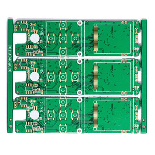
Fr4 Copper Clad Laminate Multilayer HDI 1.0mm PCB For Mobile Phone
Quick detail:
Material:Fr4 |
Layer:4 |
Surface finish:immersion gold |
Copper weight:1oz |
Board size:4.5*3cm |
Total thickness:1.6mm |
Min line width and space:3mil |
Min hole: 0.15mm |
Name:High density Interconnector printed circuit boards |
HDI PCB information:
HDI is an abbreviation of High Density Interconnector . It is a
kind of circuit board which uses micro blind buried hole
technology. HDI is a compact product designed for small-capacity
users.
Microvias are used as the interconnects between layers in high
density interconnect (HDI) substrates and printed circuit boards
(PCBs) to accommodate the high input/output (I/O) density of
advanced packages. Driven by portability and wireless
communications, the electronics industry strives to produce
affordable, light, and reliable products with increased
functionality. At the electronic component level, this translates
to components with increased I/Os with smaller footprint areas
(e.g. flip-chip packages, chip-scale packages, and direct chip
attachments), and on the printed circuit board and package
substrate level, to the use of high density interconnects (HDIs)
(e.g. finer lines and spaces, and smaller vias).
IPC standards define microvias as blind or buried vias with a
diameter equal to or less than 150 μm. With the advent of
smartphones and hand-held electronic devices, microvias have
evolved from single-level to stacked microvias that cross over
multiple HDI layers. Sequential build-up (SBU) technology is used
to fabricate HDI boards. The HDI layers are usually built up from a
traditionally manufactured double-sided core board or multilayer
PCB. The HDI layers are built on both sides of the traditional PCB
one by one with microvias. The SBU process consists of several
steps: layer lamination, via formation, via metallization, and via
filling. There are multiple choices of materials and/or
technologies for each step.
Microvias can be filled with different materials and
processes:filled with epoxy resin (b-stage) during a sequential
lamination process step; filled with non-conductive or conductive
material other than copper as a separate processing step; plated
closed with electroplated copper; screen printed closed with a
copper paste. Buried microvias are required to be filled, while
blind microvias on the external layers usually do not have any fill
requirements.A stacked microvia is usually filled with
electroplated copper to make electrical interconnections between
multiple HDI layers and provide structural support for the outer
level(s) of the microvia or for a component mounted on the
outermost copper pad.
HDI PCB application:
Electronic design continues to improve the performance of the
whole, while also trying to reduce its size. From mobile phones to
smart weapons, small portable products, "small" is always the same
pursuit. High-density integration (HDI) technology can make the end
product design more compact, while meeting the electronic
performance and efficiency of higher standards. HDI is widely used
in mobile phones, digital cameras, MP3, MP4, computers, automotive
electronics and other digital products, among which the most widely
used mobile phones. HDI board generally used to build-up
manufacturing, the more the number of layers, the higher the
technical grade plate. Ordinary HDI board is basically a laminated,
high-level HDI with 2 or more layers of technology, while using
stacked holes, electroplating fill, laser drilling and other
advanced direct PCB technology. High-end HDI board is mainly used
in 3G mobile phones, advanced digital cameras, IC board and so on.
Advantages of HDI PCB:
Can reduce the cost of PCB
Increased Line Density: Interconnecting Traditional Boards to Parts
With better electrical performance and signal correctness
Reliability is better
Can improve the thermal properties
Can improve the radio frequency interference / electromagnetic
interference / electrostatic discharge (RFI / EMI / ESD)
Increase design efficiency
Parameter technology of HDI PCB:
Feature | Technical specification |
Number of layers | 4 – 22 layers standard, 30 layers advanced |
Technology highlights | Multilayer boards with a higher connection pad density than
standard boards, with finer lines/spaces, smaller via holes and
capture pads allowing microvias to only penetrate select layers and
also be placed in surface pads. |
HDI builds | 1+N+1, 2+N+2, 3+N+3,4+N+4, any layer in R&D |
Materials | FR4 standard, FR4 high performance, Halogen free FR4, Rogers |
Delivery | DHL,Fedex,UPS |
Copper weights (finished) | 18um – 70um |
Minimum track and gap | 0.075mm / 0.075mm |
PCB thickness | 0.40mm – 3.20mm |
Maxmimum dimensions | 610mm x 450mm; dependant upon laser drilling machine |
Surface finishes available | OSP, ENIG, Immersion tin, Immersion silver, Electrolytic gold, Gold
fingers |
Minimum mechanical drill | 0.15mm |
Minimum laser drill | 0.10mm standard, 0.075mm advanced |
FR4 PCBs are known for their excellent thermal stability, high
mechanical strength, and resistance to moisture and chemicals.
These properties make them suitable for a wide range of
applications, including consumer electronics, telecommunications,
automotive, industrial equipment, and more.
The FR4 material consists of a thin layer of copper foil laminated
onto a substrate made of woven fiberglass cloth impregnated with
epoxy resin. The copper layer is etched to create the desired
circuit pattern, and the remaining copper traces provide the
electrical connections between components.
The FR4 substrate offers good dimensional stability, which is
important for maintaining the integrity of the circuitry over a
wide range of temperatures. It also has low electrical
conductivity, which helps prevent short circuits between adjacent
traces.
In addition to its electrical properties, FR4 has good flame
retardant properties due to the presence of halogenated compounds
in the epoxy resin. This makes FR4 PCBs suitable for applications
where fire safety is a concern.
Overall, FR4 PCBs are widely used in the electronics industry due
to their excellent combination of electrical performance,
mechanical strength, thermal stability, and flame retardancy.