Shenzhen Tecircuit Electronics Limited
TECircuit Electronic Co.,Ltd founded in 2004, is a
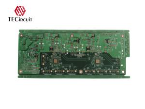
proficient PCB&PCBA manufacturer as a National High-Tech
Enterprise.Based on our PCB factory in Huizhou city, Guangdong, we
produce 1-40L PCB precisely and densely. Along with our 8 SMT
lines, we are remarkable in PCBA among vast territory. Focus on
domestic and overseasour products have been promoted to over 30
countries and areas, and accumulated rich experience invarious
industries including but not limited to Telecommunication, 5G, loT,
Medical, Industrial Control.Automotive.Instrumentation. aviation
and defence.To be reliable and high-quality, we have passed UL,ISO
9001, ISO 14001, ISO 13485, ITAF 16949 andcomplied with ROHS and
REACH. We are eager to innovate and have acquired more than 20
patentsThinking at our partners side, we devote ourselves into
one-stop service in PCB Manufacturing, PCB Assembly, Components
Sourcing for 16 years.