

Electronics SMT PCB SMD Assembly Components 12 Layer OEM
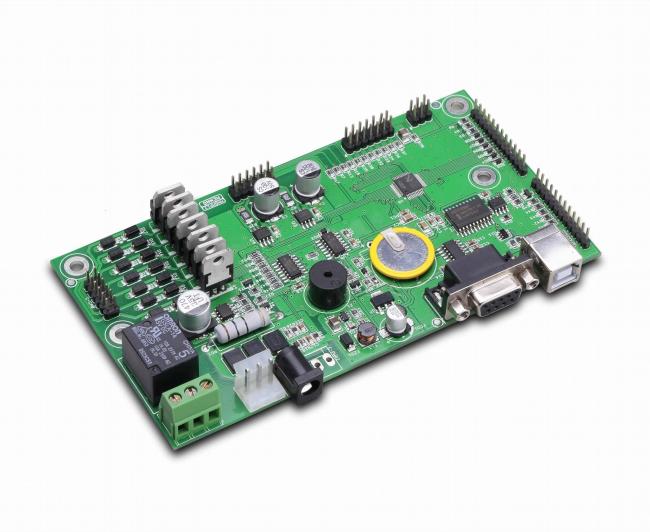
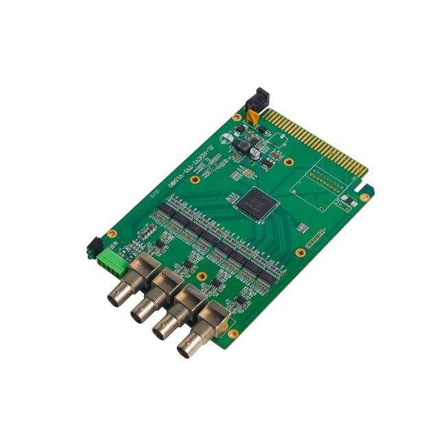
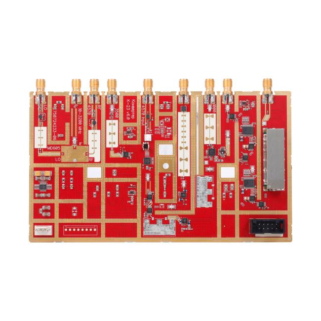
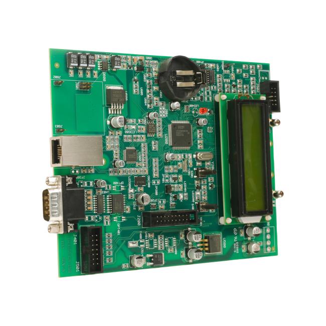
Electronics PCB Components Assembly and SMT Assembly Product Specifications Attribute Value Layer 12 Layer Material FR4 Board Thickness 2.5mm Surface Finish Immersion Gold Pin Space 0.25mm Application Electronic Products 12 Layer Industrial Control SMT PCB Assembly Electronics PCB Components Assembly (also called PCBA - Printed Circuit Board Assembly) is the process of mounting and soldering electronic components onto a bare PCB to create a functional circuit board. This
| Attribute | Value |
|---|---|
| Layer | 12 Layer |
| Material | FR4 |
| Board Thickness | 2.5mm |
| Surface Finish | Immersion Gold |
| Pin Space | 0.25mm |
| Application | Electronic Products |
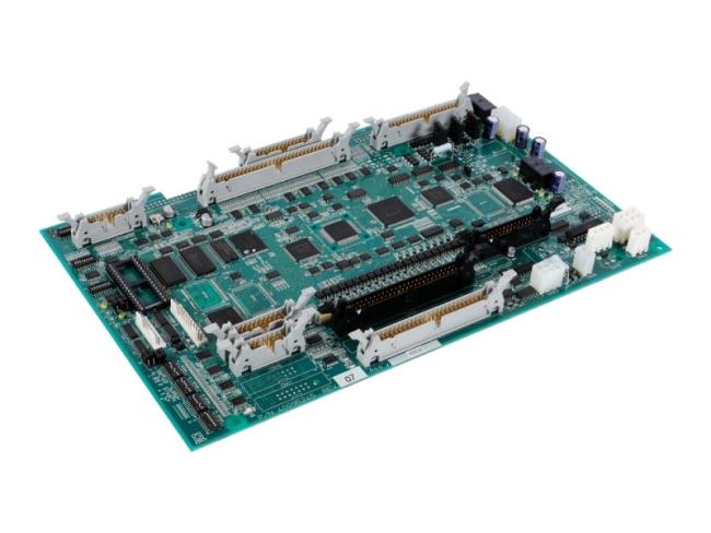
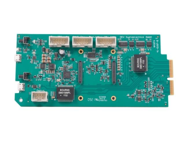
Electronics PCB Components Assembly (also called PCBA - Printed Circuit Board Assembly) is the process of mounting and soldering electronic components onto a bare PCB to create a functional circuit board. This process transforms a blank PCB into a working electronic device, such as a smartphone, computer, or IoT gadget.
- Passive Components (resistors, capacitors, inductors)
- Active Components (ICs, transistors, diodes)
- Electromechanical Parts (connectors, switches, relays)
There are two primary assembly techniques:
- Components are placed directly onto PCB pads
- Process Steps:
- Solder Paste Application (using a stencil)
- Pick-and-Place Machine (automated component placement)
- Reflow Soldering (melts solder paste in an oven)
- Best for: High-density, compact designs (e.g., smartphones, laptops)
- Components have leads inserted into drilled holes
- Process Steps:
- Manual/Automated Insertion of components
- Wave Soldering (solder flows over the board)
- Best for: High-power, durable applications (e.g., industrial equipment, automotive)
Combines both methods for complex designs.
| Step | Description |
|---|---|
| 1. Solder Paste Printing | A stencil applies solder paste to PCB pads |
| 2. Component Placement | Pick-and-place machines position SMD components |
| 3. Reflow Soldering | Heats PCB to melt solder and form connections |
| 4. Through-Hole Insertion | THT components are manually/machine-inserted |
| 5. Wave Soldering (THT) | Solder bonds THT components to the board |
| 6. Inspection & Testing | AOI (Automated Optical Inspection), X-ray (for BGAs), functional testing |
| 7. Conformal Coating (Optional) | Protects PCB from moisture, dust, and corrosion |
DQS Electronic Group is one of the leading EMS companies in China, providing PCB design, PCB manufacturing, PCB assembly service and testing. Welcome to send us your Gerber file to get a free quotation. Our email: [email protected]
| PCB Assembly Capability | ||
|---|---|---|
| Item | Normal | Special |
| SMT Assembly | PCB(used for SMT) specification | |
| Length and Width( L* W) | Minimum: L≥3mm, W≥3mm Maximum: L≤800mm, W≤460mm |
L<2mm L>1200mm, W>500mm |
| Thickness( T) | Thinnest: 0.2mm Thickest: 4 mm |
T<0.1mm T>4.5mm |
| SMT components specification | Outline Dimension Min size: 0201(0.6mm*0.3mm) Max size: 200 * 125 Component thickness: T≤15mm |
01005(0.3mm*0.2mm) 200 * 125 6.5mm<T≤15mm |
| QFP,SOP,SOJ (multi pins) | Min pin space: 0.4mm | 0.3mm≤Pitch<0.4mm |
| CSP/ BGA | Min ball space: 0.5mm | 0.3mm≤Pitch<0.5mm |
| DIP Assembly | PCB specification Length and Width( L* W) Minimum: L≥50mm, W≥30mm Maximum: L≤1200mm, W≤450mm Thickness( T) Thinnest: 0.8mm Thickest: 3.5mm |
L<50mm L≥1200mm, W≥500mm T<0.8mm T>2mm |
- Owned PCBA factories 15,000 ㎡
- 13 fully automatic SMT lines
- 4 DIP assembly lines
- IATF, ISO, IPC, UL standards
- Online SPI, AOI, X-Ray Inspection
- The qualified rate of products reach 99.9%
- 24H reply your inquiry
- Perfect after-sales service system
- From prototype to mass production
Recommended Products
 Video
Video
Video
Video
Video
Video
Video
Video