


Hdi Rigid Flex Pcb Hdi Technology 10Layer High Density Interconnect Pcbs
High Precision Multilayer PCB Printed Circuit Boards Blind And Buried Via/Flexible PCB Hdi Pcb High Thermal Reliability Ultra-Low Loss High Speed Digital Halogen-Free RoHS Compliant Lead-Free High Tg 1 . Descriptions: What is a HDI PCB? HDI stands for High Density Interconnector. A circuit board which has a higher wiring density per unit area as opposed to conventional board is called as HDI PCB. HDI PCBs have finer spaces and lines, minor vias and capture pads and higher
High Precision Multilayer PCB Printed Circuit Boards Blind And Buried Via/Flexible PCB Hdi Pcb
- High Thermal Reliability
- Ultra-Low Loss
- High Speed Digital
- Halogen-Free
- RoHS Compliant
- Lead-Free High Tg
1 . Descriptions:
What is a HDI PCB?
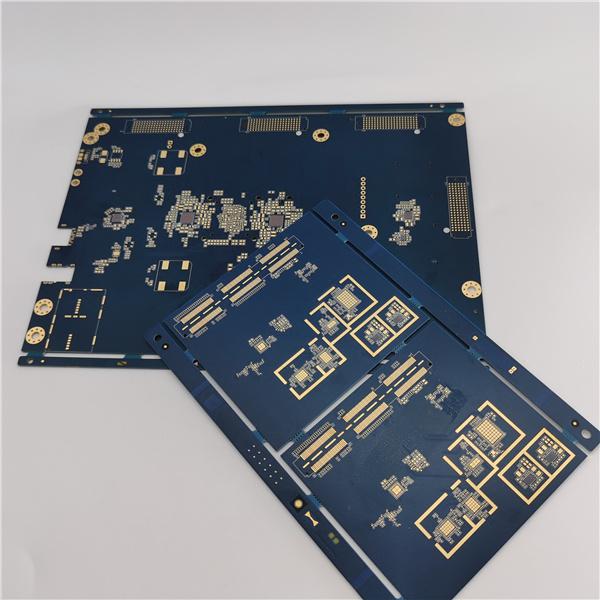
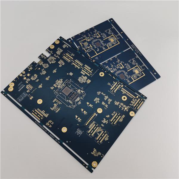
HDI stands for High Density Interconnector. A circuit board which has a higher wiring density per unit area as opposed to conventional board is called as HDI PCB. HDI PCBs have finer spaces and lines, minor vias and capture pads and higher connection pad density. It is helpful in enhancing electrical performance and reduction in weight and size of the equipment. HDI PCB is the better option for high-layer count and costly laminated boards.
Regarding the electrical needs of high-speed signal, the board should have various features i.e. high-frequency transmission capability, impedance control, decreases redundant radiation, etc. The board should be enhanced in the density because of the miniaturization and arrays of the electronic parts. In addition, to the result of the assembling techniques of leadless, fine pitch package and direct chip bonding, the board is even featured with exceptional high-density.
Innumerable benefits are associated with HDI PCB, like high speed, small size and high frequency. It is the primary part of portable computers, personal computers, and mobile phones. Currently, HDI PCB is extensively used in other end user products i.e. as MP3 players and game consoles, etc.
2 . Specifications:
| Name | 10L Tablet computer mainboard |
| Number of Layers | 10 |
| Quality Grade | IPC 6012 Class 2,IPC 6012 Class 3 |
| Material | EM370 |
| Thickness | 0.7mm |
| Min Track/Spacing | 50um/60um |
| Min Hole Size | Laser 75um; Drilling size 200um |
| Solder Mask | Green |
| Silkscreen | White |
| Surface Finish | Immersion gold,OSP |
| Finished Copper | 12um |
| Production time | 10-21 working days |
| Lead time | 2-3 days |
3. Advantages:
The most common reason for using HDI technology is a significant increase in packaging density. The space obtained by finer track structures is available for components. Besides, overall space requirements are reduced will result in smaller board sizes and fewer layers.
Usually FPGA or BGA are available with 1mm or less spacing. HDI technology makes routing and connection easy, especially when routing between pins.
Recommended Products
