


Multi Layer HDI PCB Board Design Surface Laminar Circuit PCB Stuffing
HDI PCB Board Multi-Layer Printed Circuit Boards Surface Laminar Circuit HDI PCB: Implementation of Blind, buried, and microvias Laser direct drilling Lower number of layers Higher component density per square inch Compatible with high pin count and low pitch packages Smaller, lighter boards with more functionality PCB Manufacture Capacity Feature Capability Service Type HDI PCB Board Multi-Layer Printed Circuit Boards Surface Laminar Circuit Quality Grade Standard IPC 2
HDI PCB Board Multi-Layer Printed Circuit Boards Surface Laminar Circuit
PCB Manufacture Capacity
| Feature | Capability |
| Service Type |
HDI PCB Board Multi-Layer Printed Circuit Boards Surface Laminar Circuit |
| Quality Grade | Standard IPC 2 |
| Number of Layers | 4 - 48ayers |
| Order Quantity | 1pc - 10000+pcs |
| Build Time | 2days - 5weeks |
| Material | FR4 standard Tg 140°C,FR4 High Tg 170°C, FR4 and Rogers combined lamination |
| Board Size | Min 6*6mm | Max 457*610mm |
| Board Thickness | 0.4mm - 3.0mm |
| Copper Weight (Finished) | 0.5oz - 2.0oz |
| Min Tracing/Spacing | 2.5mil/2.5mil |
| Solder Mask Sides | As per the file |
| Solder Mask Color | Green, White, Blue, Black, Red, Yellow |
| Silkscreen Sides | As per the file |
| Silkscreen Color | White, Black, Yellow |
| Surface Finish | HASL - Hot Air Solder Leveling Lead Free HASL - RoHS ENIG - Electroless Nickle/Immersion Gold - RoHS Immersion Silver - RoHS Immersion Tin - RoHS OSP - Organic Solderability Preservatives - RoHS |
| Min Annular Ring | 4mil, 3mil - laser drill |
| Min Drilling Hole Diameter | 6mil, 4mil - laser drill |
| Max Exponents of Blind/Buried Vias | stacked vias for 3 layers interconnected, staggered vias for 4 layers interconnected |
| Other Techniques | Flex-rigid combination Via In Pad Buried Capacitor (only for Prototype PCB total area ≤1m²) |
What is HDI technology?
HDI Boards – High Density Interconnect. HDI boards, one of the fastest growing technologies in PCBs, are now available at Epec. HDI Boards contain blind and/or buried vias and often contain microvias of . 006 or less in diameter. They have a higher circuitry density than traditional circuit boards.
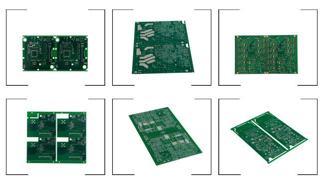
Shenzhen Yideyi Technology Co., Ltd was established in 2019, we focus on the manufacturing and development of single-layer, double-layer and multi-layer printed circuit boards.With application in the fields of telecommunications, medical equipment, computers, automobiles, and textile machine ect.
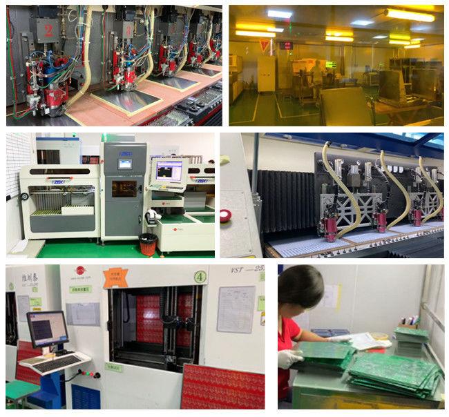
FAQs:
1, Do you offer quick turn PCB Assembly ?
Yes, we offer 24 hours quick turn PCB Assembled Solution without sacrifice the quality of the PCB Board.
2, Do you offer X-Ray capability ?
Yes, we inspect the boards using X-ray and therefore offer total reliability.
3, Do you offer conformal coating service ?
Yes, conformal coating is a part of our value-added services.
4, Do you offer testing service ?
Yes, we offer robust functional testing that adds to the product reliability.
5, Do you offer IPC 610 or J-STD Quality inspections ?
Absolutely, we offer these inspections as per client requirements.
6, Do you offer first article inspection ?
Yes, basis client requirements, we are well equipped to offer first article inspection.
7, What is your standard turnatound time for PCB Assembly ?
Our standard turnaround time for PCB Assembly is 3 weeks.
Recommended Products
