


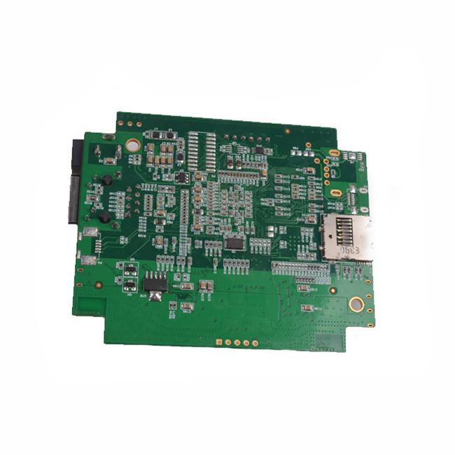
Costomized Electronic PCB Assembly HASL Surface For GPS Tracker GPS Module Device
Costomized Electronic PCB PCBA for GPS tracker GPS module device Article Description Capability Sercive PCB and SMT assembly with one-stop service Material Laminate materials FR4, high TG FR4, high frequency, alum, FPC Board cutting Number of layers 1-48 Min.thickness for inner layers (Cu thickness are excluded) 0.003”(0.07mm) Board thickness Standard (0.1-4mm±10%) Min. Single/Double:0.008±0.004” 4layer:0.01±0.008” 8layer:0.01±0.008” Bow and twist 7/1000 Copper weight Outer
Costomized Electronic PCB PCBA for GPS tracker GPS module device
|
Article |
Description |
Capability |
|
|
Sercive |
PCB and SMT assembly with one-stop service |
||
|
Material |
Laminate materials |
FR4, high TG FR4, high frequency, alum, FPC |
|
|
Board cutting |
Number of layers |
1-48 |
|
|
Min.thickness for inner layers (Cu thickness are excluded) |
0.003”(0.07mm) |
||
|
Board thickness |
Standard |
(0.1-4mm±10%) |
|
|
Min. |
Single/Double:0.008±0.004” |
||
|
4layer:0.01±0.008” |
|||
|
8layer:0.01±0.008” |
|||
|
Bow and twist |
7/1000 |
||
|
Copper weight |
Outer Cu weight |
0.5-4 0z |
|
|
Inner Cu weight |
0.5-3 0z |
||
|
Drilling |
Min size |
0.0078”(0.2mm) |
|
|
Drill deviation |
±0.002″(0.05mm) |
||
|
PTH hole tolerance |
±0.002″(0.005mm) |
||
|
NPTH hole tolerance |
±0.002″(0.005mm) |
||
|
Solder mask
|
Color |
Green,white,black,red,blue… |
|
|
Min solder mask clearanace |
0.003″(0.07mm) |
||
|
Thickness |
(0.012*0.017mm) |
||
|
Silkscreen |
Color |
white,black,yellow,blue… |
|
|
Min size |
0.006″(0.15mm) |
||
|
E-test |
Function Test |
100% Functional test |
|
|
PCBA Testing |
X-ray,AOI Test,Functional test |
||
|
Pcb assembly |
one-stop service electronic manufacxturer service |
||
|
Component sourcing |
Yes |
||
|
Certificate |
IATF16949,ISO9001 |
||
|
Delivery time: |
PCB |
3-12days |
|
|
PCBA |
8-20days |
||
|
Tolerance of pcb |
±5% |
||
|
Max size of finish board |
450*450mm |
||
|
MOQ |
NO MOQ (1pcs) |
||
|
Surface Finish |
HASL,ENIG,immersion silver,immersion tin,OSP… |
||
|
PCB outline |
Square,circle,irregular(with jigs) |
||
|
package |
QFN,BGA,SSOP,PLCC,LGA |
||
|
Sub-assembly |
Plastic,metal,screen |
||
OEM/ODM/EMS Services For PCBA
· PCBA, PCB Board assembly: SMT & PTH & BGA
· PCBA and enclosure design
· Components sourcing and purchasing
· Quick prototyping
· Plastic injection molding
· Metal sheet stamping
· Final assembly
· Test: AOI, In-Circuit Test (ICT), Functional Test (FCT)
· Custom clearance for material importing and product exporting
PCB Manufacturing Lead Time
| Layer/Days | Sample(Normal) | Sample(Fast) | Mass Production |
| Single/Double | 2-3days | 24hours | 5-7days |
| Four Layer | 7-10days | 3days | 7-10days |
| Six Layer | 7-10days | 5days | 13-15days |
| Eight Layer | 15-20days | 7days | 15-20days |
PCB Assembly Capabilities
| Turnkey PCBA | PCB+components sourcing+assembly+package |
| Assembly details | SMT and Thru-hole, ISO lines |
| Lead Time | Prototype: 15 work days. Mass order: 20~25 work days |
| Testing on products | Flying Probe Test, X-ray Inspection, AOI Test, functional test |
| Quantity | Min quantity: 1pcs. Prototype, small order, mass order, all OK |
| Files we need | PCB: Gerber files(CAM, PCB, PCBDOC) |
| Components: Bill of Materials(BOM list) | |
| Assembly: Pick-N-Place file | |
| PCB panel Size | Min size: 0.25*0.25 inches(6*6mm) |
| Max size: 20*20 inches(500*500mm) | |
| PCB Solder Type | Water Soluble Solder Paste, RoHS lead free |
| Components details | Passive Down to 0201 size |
| BGA and VFBGA | |
| Leadless Chip Carriers/CSP | |
| Double-sided SMT Assembly | |
| Fine Pitch to 0.8mils | |
| BGA Repair and Reball | |
| Part Removal and Replacement | |
| Component package | Cut Tape,Tube,Reels,Loose Parts |
| PCB assembly process |
Drilling-----Exposure-----Plating-----Etaching & Stripping-----Punching-----Electrical Testing-----SMT-----Wave Soldering-----Assembling-----ICT-----Function Testing-----Temperature & Humidity Testing |
PCBA Picture
Recommended Products
 Video
Video